Industrial Manufacturing
Demand for 300-Millimeter Chips Fuels Global Semiconductor Manufacturing Investments
In the U.S. alone, over $4 billion in capital spending is planned to be invested by semiconductor manufacturers in 2005 - Includes 2005 U.S. Semiconductor Manufacturing Project Distribution Chart
Released Wednesday, November 03, 2004

Researched by Industrialinfo.com (Industrial Information Resources, Incorporated; Houston, Texas). Semiconductor manufacturers are expected to invest significant amounts of money in their manufacturing and research facilities in 2005. Most of the investment is being fueled by demand for 300-millimeter (12-inch diameter) silicon wafers. Manufacturing with 300-mm wafers substantially increases the ability to produce semiconductors at a lower cost then with the current standard 200-mm (8-inch) wafers. The surface area of a 300-mm wafer is 225% larger than a 200-mm wafer and is able to produce 240% more individual chips. The larger wafer also reduces the production cost per chip and uses fewer resources. For example, a 300-mm wafer manufacturing facility will use 40% less energy and water than a 200-mm production facility.
In the U.S. alone, Industrialinfo.com has identified over $4 billion in capital project spending to be invested by semiconductor manufacturers in 2005. As of November 2004, this is approximately $1 billion less than what is forecast to be spent throughout the remainder of 2004. Currently, of the eleven total projects identified for 2005, five are grassroot plants and their total investment value (TIV) ranges from $1 million to $300 billion.
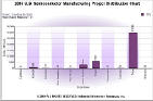 Click on the image at right to view the 2005 U.S. Semiconductor Manufacturing Project Distribution Chart.
The largest proposed semiconductor project for 2005 is a new 300-millimeter silicon wafer production plant in Richardson, Texas. Texas Instruments (TI) (NASDAQ:TXN) (Dallas, Texas) plans to construct a 2 million square foot facility on a 92-acre site. The plant will include a 220,000 square foot clean room that will utilize TI's 65 nanometer (nm) process technology to build some of the worlds most advanced semiconductor designs on 300-mm wafers. Texas Instruments has announced that they will hold a groundbreaking ceremony on November 18, 2004. Initial plans were for construction to begin Spring 2005, but now the construction schedule has moved forward. In the same manner as they constructed their first 300-mm facility, DMOS6 in Dallas, Texas Instruments plans to construct the building and infrastructure ahead of market demand with phases of equipment installation occurring as demand dictates. Once completed in late 2006 the fabrication facility or "fab," will be one of the most advanced semiconductor manufacturing facilities in the world, producing a wide range of digital signal processing (DSP) and analog-based system-on-chip (SoC) devices for wireless, broadband and digital consumer applications.
Another significant investment occurring in the semiconductor industry is Cree Industries Incorporateds (NASDAQ:CREE)Durham, North Carolina) plans to invest a minimum of $300 million to construct a manufacturing and research facility in the Research Triangle Park area near the company's current headquarters. The project is expected to begin construction next year and Cree expects to employ approximately 300 people upon completion in 2006.
Siltronic AG (Munich, Germany), a division of WACKER Group (Munich, Germany), is scouting sites for a $600 million fabrication plant to produce 300-mm wafers. In the U.S., Siltronic is considering possible sites in Portland, Oregon, near its existing plant. Other potential sites are in Germany, Singapore, and Thailand. Siltronic has recently started a 300-mm silicon wafer production line in Freiberg, Saxony. A final decision on the location of the new plant is expected by the end of 2004, with construction following in early Summer 2005.
Substantial investments by semiconductor companies are taking place abroad as well, especially in China because of its explosive growth. Hynix Semiconductor Incorporated (Seoul, South Korea) has received approval to construct two wafer fabs in China with STMicroelectronics NV (Geneva, Switzerland). One of the plants will produce 200-mm and the other will make 300-mm diameter wafers. Under the terms of the joint venture, each party would invest $500 million plus borrow an additional $1 billion from China. The plants will be constructed in phases with the 200-mm fab being built first and the 300-mm fab following shortly after. These facilities would help Hynix increase its production capacity of DRAM and avoid paying the duties that are imposed on chips made in South Korea.
The first 300-mm plant in China began operation on September 25, 2004 and is owned and operated by Semiconductor Manufacturing International Corporation (SMIC) (Shanghai, China) and manufactures DRAM for Infineon Technologies AG (Munich, Germany) and Elpida Memory Incorporated (Tokyo, Japan). SMIC has plans to construct three 300-mm plants in Beijing over the next several years.
Domestic semiconductor manufactures are moving towards a period of uncertainty, with excess inventories and China once again becoming a source of low cost imports. They must continue to invest in new plants and upgrade existing ones, while continuing to develop cutting edge technologies and be as efficient as possible. With demand coming from so many different industries and for so many different applications, companies are continually challenged to develop new manufacturing process and techniques to meet consumer demands.
View Plant Profiles - 1061309 1064159 1063876
View Project Reports - 01009482 15001951 22001026
Industrialinfo.com is the leading provider of global industrial market research. We specialize in helping companies develop information solutions to maximize their sales and marketing efforts.
/news/article.jsp
false
Want More IIR News Intelligence?
Make us a Preferred Source on Google to see more of us when you search.
Add Us On GoogleAsk Us
Have a question for our staff?
Submit a question and one of our experts will be happy to assist you.

Forecasts & Analytical Solutions
Where global project and asset data meets advanced analytics for smarter market sizing and forecasting.
Explore Our Solutions
PECWeb Global Market Intelligence Platform
Identify opportunities, anticipate change, and execute with confidence. PECWeb connects the industrial intelligence you need, from projects and assets to operational events, all in one platform.
Discover PecwebIndustry Intel
-
Brazil: Efficiency, Innovation, and Opportunities in the Food & Beverage IndustryPodcast Episode / Jun 12, 2026
-
2026-2027 Investment Radar for Mexico, Central America & the CaribbeanPodcast Episode / May 29, 2026
-
Innovations Shaping the Next Era of Power GenerationPodcast Episode / May 22, 2026
-
The Role of Contract Manufacturing in Global Pharma GrowthPodcast Episode / May 8, 2026
-
2026 North American Labor OutlookPodcast Episode / Apr 24, 2026